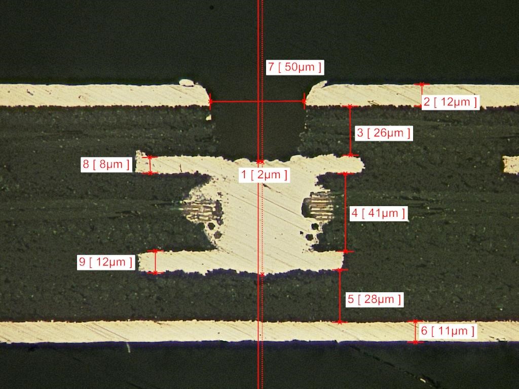
This case study focuses on the challenges and solutions that we implemented to design complex HDI boards with stacked vias.
Case study: 8 and 14-layer HDI with Stacked Vias
Case study: 8 and 14-layer HDI with Stacked Vias
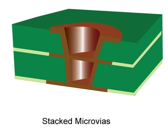
Designing Staggered and Stacked Vias
Designing HDI PCBs: The Requirements, Advantages and Complexities

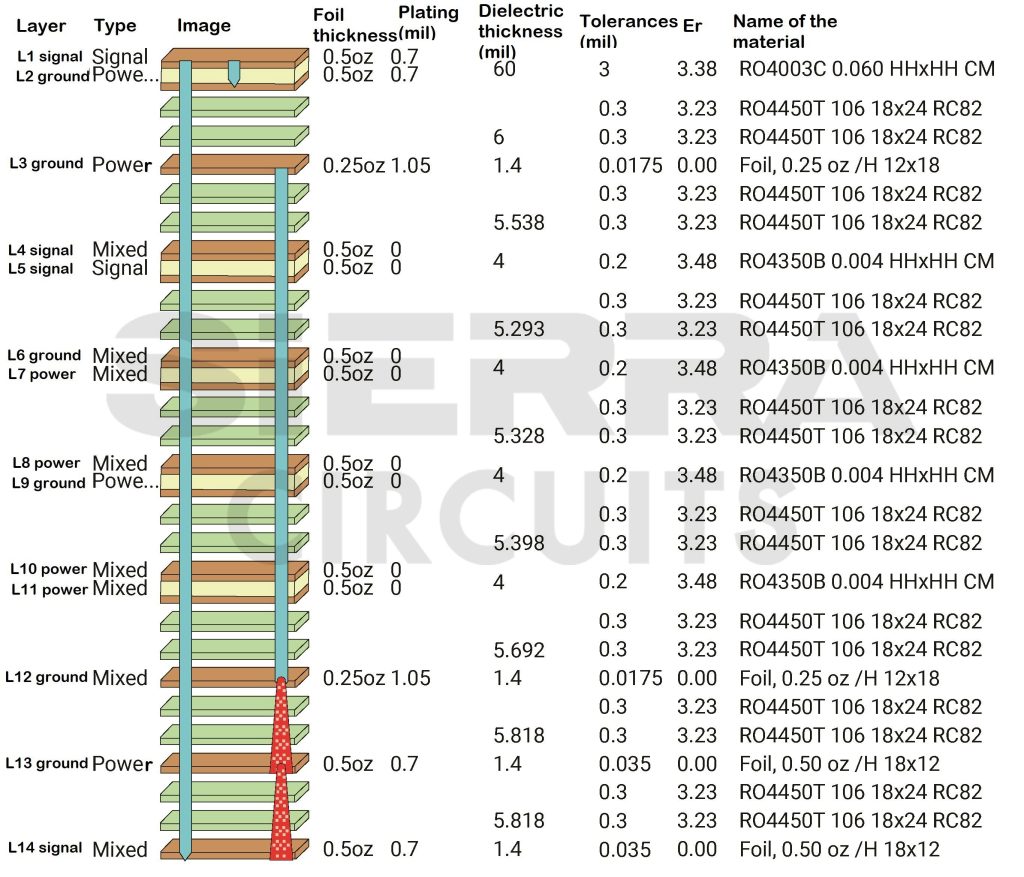
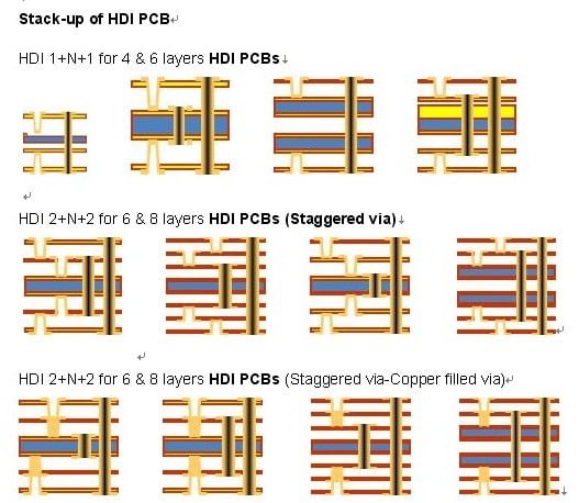
HDI board stack-ups
Case study: 8 and 14-layer HDI with Stacked Vias

Ultimate HDI PCB Manufacturer in China PCBTok

Understanding Proper PCB Design (Part 2) - Circuit Cellar
Technologies and processes at ILFA: Sophisticated HDI design in PCB production - ILFA Feinstleiter Technologie
PDF) HDI via structures effect on PCB design flexibility, constraints and cost
HDI PCB: Pushing the Limits of Your Electronics - MOKO Technology

An in-depth analysis on PCB stackup