Share

PCB Design Considerations and Guidelines for 0.4mm and 0.5mm WLPs
Working With BGAs: Design And Layout
FET Test Chips, Optimized for 2D Materials, Platinum
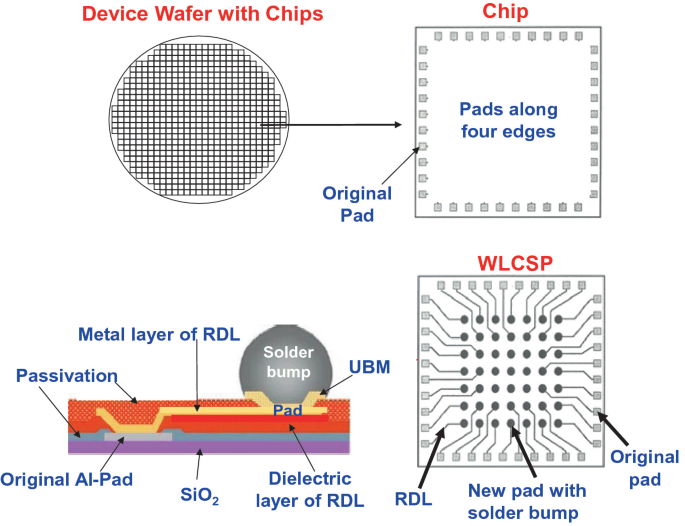
Fan-In Wafer/Panel-Level Chip-Scale Packages

Micromachines, Free Full-Text

What is Pad to Pad (PP) ?
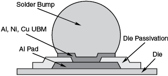
Challenges Grow For Creating Smaller Bumps For Flip Chips

Challenges and recent prospectives of 3D heterogeneous integration

PCB pad design principles
What is Pad to Pad (PP) in PCB ?. Pad to Pad or PP is an important

Design and characterization of a copper-pillar flip chip test vehicle for small form-factor packages using 28nm ELK die and bump-on-trace (BOT)
Related products

You may also like